Eagle
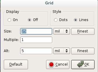
Grid
It's possible to configure a grid to use to snap elements to, it's also possible to move part in a finer way
holding down the Alt button (this make the part snap to the alternative grid)
Text
The text goes on the silkscreen, represented by the two layers tPlace and bPlace (respectively
layer 21 and 22)
Images
It's possible to import a BMP image file running run import-bmp.ulp from the console;
the image should have only two colors (probably you are converting from a different format, so
be aware of alpha channel, number of colors, etc...).
Import it using the dialog into the correct layer.
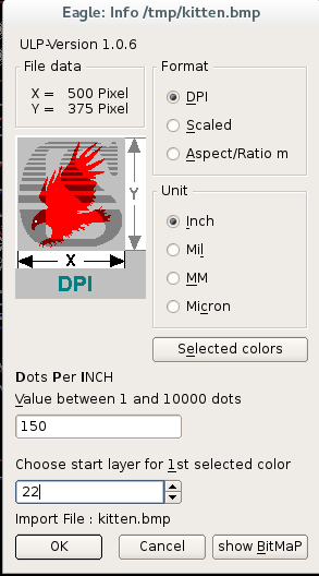
My advice is to create a new fake device with the image imported as package: in this way you can move and do actions on it more easily.
Dimensions
The PCB size is determined from the outline of the layer 20.
Creating a new part
Eagle requires three things to get an IC into the library:
- Package (also known as a footprint)
- Symbol (the schematic symbol)
- Device (mapping them together)
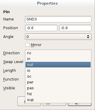
It's possible to indicate in the symbol section what use have the various pins, simply open the info
window for the pin and then select the correct indication in the direction section
Placing elements
Once an element is added to the schematics it's placed also on the board window and it's possible to move around.
Probably the label and value of the element will be placed in a position that is not correct, to correct
that is possible to use the smash action from the contextual menu: this will de-connect the label and the
value that can be moved and edited separately.
Tracing
You can use a trick to hide the GND wires: select with the info tool the wire and
then check the box Airwires hidden.
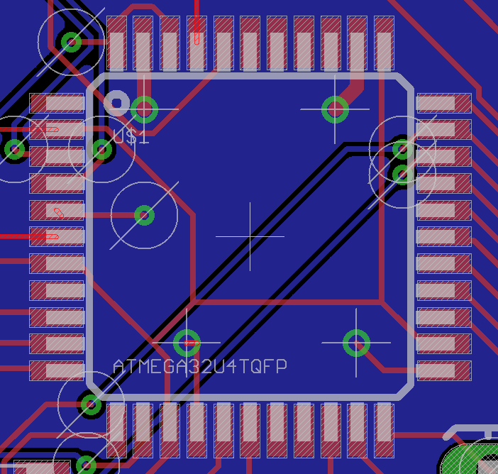
Some chips have GND and VCC pins distribuited randomly along the sides and can be difficultous to be
able to route all of them, so it's possible to route to the GND using vias connected directly to the a GND
plane; below an image showing an example with an ATMEGA32U4 chip
In some cases you are not able to see where the missing airwires to route are, a epic trick is to zoom out a lot and then click to the routing tool, at this point the missing piece will show magically.
There is also a zoomunrouted.ulp that zooms in on any place that is unconnected. It is a standard part of our PCB pre-flight.
SCRIPTS
Some usefull command to quick show/hide layers (source)
#default visible layers
DISPLAY NONE 1 16 17 18 19 20 21 22 23 24 25 26 39 40 41 42 48 49 50 51 52 56 101 102 104 116 121 122 151 254;
display none 16 17 18 19 22 24 26 30;
display none 1 17 18 19 20 21 23 25 51;
run find.ulp