Transistors
Have three pins named base/gate, collector/source and emitter/drain
MOSFET is voltage controlled. While BJT is current controlled,
- The collector must be more positive than the emitter
- the base-emitter and base-collector circuits behave like diodes
- where is tipically about 100
the parameter is highly dependent on temperature, current, etc.. so a circuit dependents on it is a bad circuit.
BJT
The common emitter amplifier configuration produces the highest current and power gain of all the three bipolar transistor configurations. This is mainly because the input impedance is LOW as it is connected to a forward biased PN-junction, while the output impedance is HIGH as it is taken from a reverse biased PN-junction.
Q-point
The Q stands for quiescent which means still, quiet or stable. The Q-point is on the DC load line and represents the current flowing in output circuit and voltage across it. In our case, they are IC and VCE. The value of current and voltage at Q-point are written as (VCEQ, ICQ).
The position of Q-point is selected according to the application of transistor.
- If transistor is to be used as switch, Q-point is in cut-off region for open switch and in saturation region for closed switch.
-
If transistor is to be operated as amplifier, Q-point is placed exactly in the middle of the DC load line. It is preferred at midpoint of DC load line so that it does not enter in other regions due change in temperature, βdc etc.
Configuration
Transistors comprise of three terminals i.e. Base, emitter and collector but when we connected it in a circuit, we require four terminals; two for the input and two for the output. To overcome this problem we make one terminal of the transistor common to both input and output terminals. The input is fed between the common terminal and one of the other two terminals while the output is obtained between the common terminal and the remaining terminal. Based on this, transistor is configured in the circuit in the following three ways:
- Common emitter (with emitter degeneracy when a resistor is used between emitter and ground)
- Common base
- Common collector
Junction capacitance
MOSFET
Variable resistor controlled by voltage: you can vary the resistence between drain and source varing the voltage applied between gate and source. The output current is not a multiplier of the input current (remind that MOSFET are all about voltage).
- : Voltage threasold between gate and source (if it's less than 5 volts then is logic level)
It's important to calculate the power (and of conseguence the heat) consumed by the formula
and with the parameter (Junction to ambient coefficient) and the following formula that calculate the power dissipated at ambient temperature when the transistor has a maximum junction temperature
If then you don't need a dissipator.
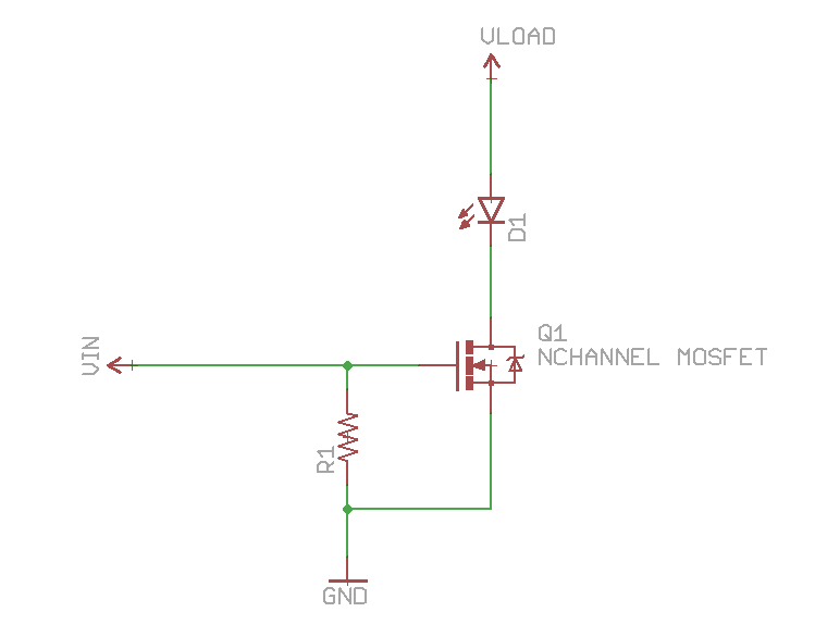
Here an example of usage
Links
- EE 320/320L Electronics I
- Tutorial by Sparkfun
- http://electronics.stackexchange.com/questions/19233/when-to-use-what-transistor
- http://blog.oscarliang.net/how-to-use-mosfet-beginner-tutorial/
- AO #10 BJTs as Transistor Switches
- AO #11 MOSFETs and How to Use Them
- Transistor biasing
- https://rheingoldheavy.com/building-things-npn-transistors/
-
281: Bipolar Transistor Switching Time Measurement video